The working and Manufacturing Process
Led lights bring rise to the bright. With astonishing uses in our day to day lives. From person to commercial, deep in the arts of industrial and modern-day residential areas. The city is always booming and running through the night. Led manufactures and distributors all across India, have found exceptional demand gaining huge market opportunities, that is now open in big cities like Pune, Ahmedabad, Secundrabad, Bangalore, Mumbai, Hyderabad, etc.
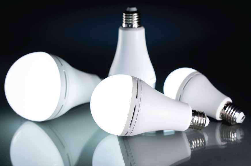
The rise of LED wholesale
The rise, start and use of modern led lightings from person to industrial usage prove energy saving 90% more than using regular incandescent lights or LED fluorescent tubes. Highlighted below, is a sum up of the most brilliant composition in the making of a fine LED lights just before it gets on its wholesaler distribution, supplies, and wholesale projects.
Making the LED semiconductor wafers:
The first thing to be made in an LED manufacturing unit is the semiconductor wafer. This is a mixture composed of GaAs, Gap or either a mix somewhere in between. This is usually determined by the specific colour of the LED that needs to be fabricated. This crystalline semiconductor is made at a very high temperature under high-pressure chambers. Arsenic, Gallium or/and phosphor gets purified while mixing within a chamber. The act of the pressure incorporated with the heat allows all components to finally mix and are forced into a particular solution in order for the components not to escape into the gas from the pressure chamber. This solution is called liquid boron oxide, which covers the mixture by layers and layers. This also helps in sealing them up, so they can easily stick together. This process is further classified as liquid encapsulation. It is also commonly known as the Czochralski Crystal growth method. Once the elements are finely tuned onto a uniformed solution, a rod gets dipped into the solution and slowly pulled out. The solution immediately cools and crystallizes at the end of that rod. It forms a long cylinder type crystal ingot at the close, or a boule of GaAs, GaAs or GaP. Just like baking a cake.
LED processing
Now, this boule is then further sliced into very fine wafers of semiconductors, this is approximately 10 mils in thickness. Or in a nutshell as thick as a garage plastic bag. These wafers then get polished until they reach a very smooth texture so that many more layers of semiconductors can be accommodated on them. Think of it in similarity to the principle of sanding a table before painting it. These wafers are still further cleaned through stringent efforts and rigorous ultrasonic and chemical cleaning process using multiple solvents. Remeber the cleaner the surface the better will the LED be.
Epitaxial layers are added
Here additional layers of semiconductor crystal are further added to the surface of the wafer just like piling layers on a cake. This is one such way to add any dopants and impurities to the crystal. These crystals are also grown by a process referred to as liquid phase epitaxy or (LPE). This technique allows epitaxial layers or otherwise such semiconductor layers to have the same crystalline orientation would get deposited onto the wafer it bathes under reservoirs of a molten solution. These reservoirs allow the dopants to get easily mixed in this procedure. The wafer will usually rest upon a graphite slide which is dragged through a particular channel under a hot container holding molten liqy\uid or as industry company and their establishments like to call it, melt. With sequential melts, many varieties of dopants can be added. They can also be added simultaneously to the melt, this creates many layers of material for different types of electronic areas, its densities, and technical specifications or requirement areas. This final deposited layer will eventually become the continuation of a wafer crystal structure.
How LPE helps LED
LPE or liquid phase epitaxy creates an outstanding uniformed layered material. Which further improves its excess growth and doping technique. These area layers can form several microns thicker in mass.
After the depositing epitaxial layers are coated it may call for a further adding dopant to help alter any specific characteristics of the diode for further classification on colour or efficiency. When additional doping is done then the wafer is again put in a high-temperature tube or furnace where once again it is immersed into a gaseous atmosphere that contains dopants like nitrogen or even zinc ammonium which are the most common ones used. Usually, nitrogen is added more to the upper layer to give the diode to make more green or yellow lights.
Adding all Light-emitting-diode Metal contacts
Metal contacts completely depend on the semiconductor wafer. The type of patterned contact is determined much in advance usually in the designed stage, this also completely depends on whether the diode is to be used in a single or combination style. The contact designs are reproduced in photoresist, which is a very light and sensitive compound of liquid which resists any type of deposited drops as the wafer spins distributing it evenly over the surface. The resist is then hardened for a brief period as the low temperature allows it to bake at 215 degrees Fahrenheit or 100 degrees Celsius. Then the master design or mask is again duplicated on the photoresist, which is placed over the wafer, thus exposing the resist to UV light. Such as in photography how a negative film is made. The exposed areas of the so-called resist getting washed away with the unexposed area that remains covering all the semiconductor layers.
Contact metal can finally be evaporated to the design while manufacturing at this process and fill up the exposed areas. This evaporation takes off under high-temperature units or chambers in a vacuum seal. This causes the chunks of metal to evaporate and when it condenses it sticks to the exposed voltage semiconductor of the wafer just like steam would tp a fog on a cold glass. The photoresist can finally be washed off with acetone leaving just the remains of the metal contact. Depending on the plan for the LED the final layers of coating may be added again on the backside of the wafer. Now any such deposited metals have to go through immense processing where the wafer is further heated to several hundred degrees and then allowed to stay in a furnace with exposed hydrogen or nitrogen flow. This happens for several hours in the making until at the end the metal and the semiconductor wafer, bind together in a chemical balance so it does not flake.
Single and multiple LEDs
Just a single 2 inch in diameter wafer can easily be produced in this form which is repeated up to six thousand times on it, this helps identify the size of a particular finish diode. These diodes are the cut separately either by cleaving, which is by snapping the semiconductor wafer along a crystal-like plane or using a diamond saw. Every single segment is commonly referred to as die. This is done by manufacturers and distributors in a seamless and impeccable process without any errors. Besides the incredible amount of procedures done to manufacture LED. An LED company or an industry in India, have found ways to make light-emitting diode available for all areas with higher quality and lower rates.
Individual dies are additionally mounted in a different way. The diode by itself is an indicator light or in some cases used for jewelry. By mounting two such metal lEDS about just two inches long, then usually the wafer gets extra coated with some metal and forms with an electrical contact that leads a resist. A small gold wire gets soldered on to the LED optical fibers head that is the wire bound with various patterns its contacts and on the surface areas of the dies the wire bonding is done with all the ends of the wire is pressed down deep into the contact metal like through a fine needle. This gold is soft enough to mold and fit the metallic surface sources. Then almost the entire assembly gets sealed into a plastic. At a point at which the wires and die get moreover suspended inside a mold that is shaped as desired clients requirements. This fiber optic lighting solution is then packaged with lens and/ or a connector at one end and the final mold is filled with epoxy or liquid plastic. This epoxy or liquid plastic is then cured and the transformation of LED is completely ready to fill up the brightness. and eliminate the dark .
LED lightings
In such ways, great LED lightings our processed till they reach our city, highways, homes and street lights, makes goods that turn illumination from the night or daily day usage in indoors, evening to sunset, dusk to dawn. LED’s have lower watt power and voltage consuming and are changing the world at sight and with new visible research and smart illumination features with technology sources and LED device that is replacing all incandescent lights and fluorescent tubes and lamp to the new LED patterned to begin a massive expansion for demand in the world.